Semiconductor processes rely on uniform, repeatable pressure to maintain yield and performance. Pressure mapping provides quantitative visibility into pressure distribution and contact conditions, enabling engineers to validate tools, optimize processes, and quickly identify sources of variation.
Heat Sink Contact Pressure
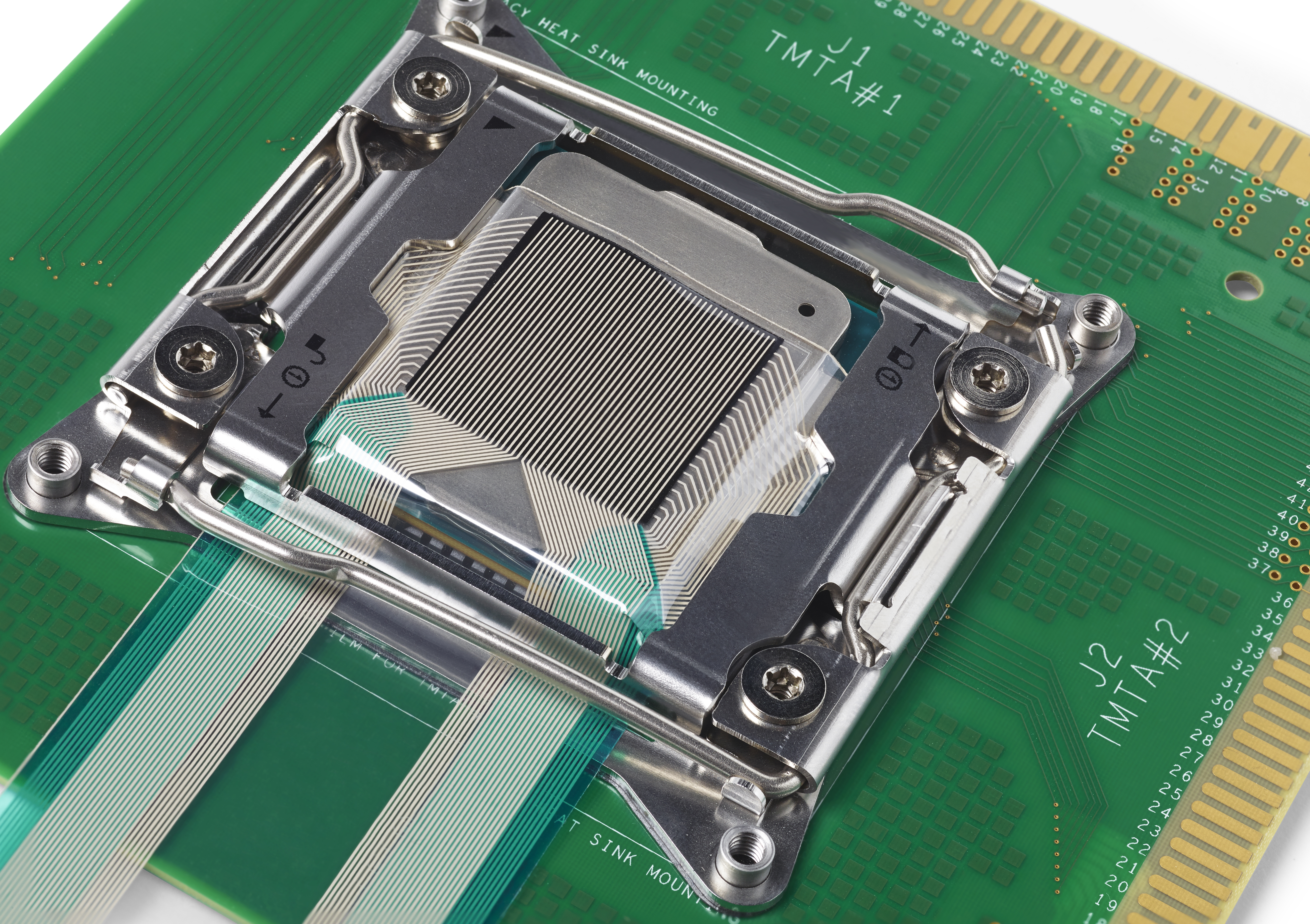
Pressure mapping reveals where a heat sink makes solid contact — and where gaps exist — so engineers can validate assembly, improve heat dissipation, and reduce thermal failures in high-density electronic systems.

Life Sciences Hardware Design
Improve life science device hardware R&D and testing with pressure mapping.
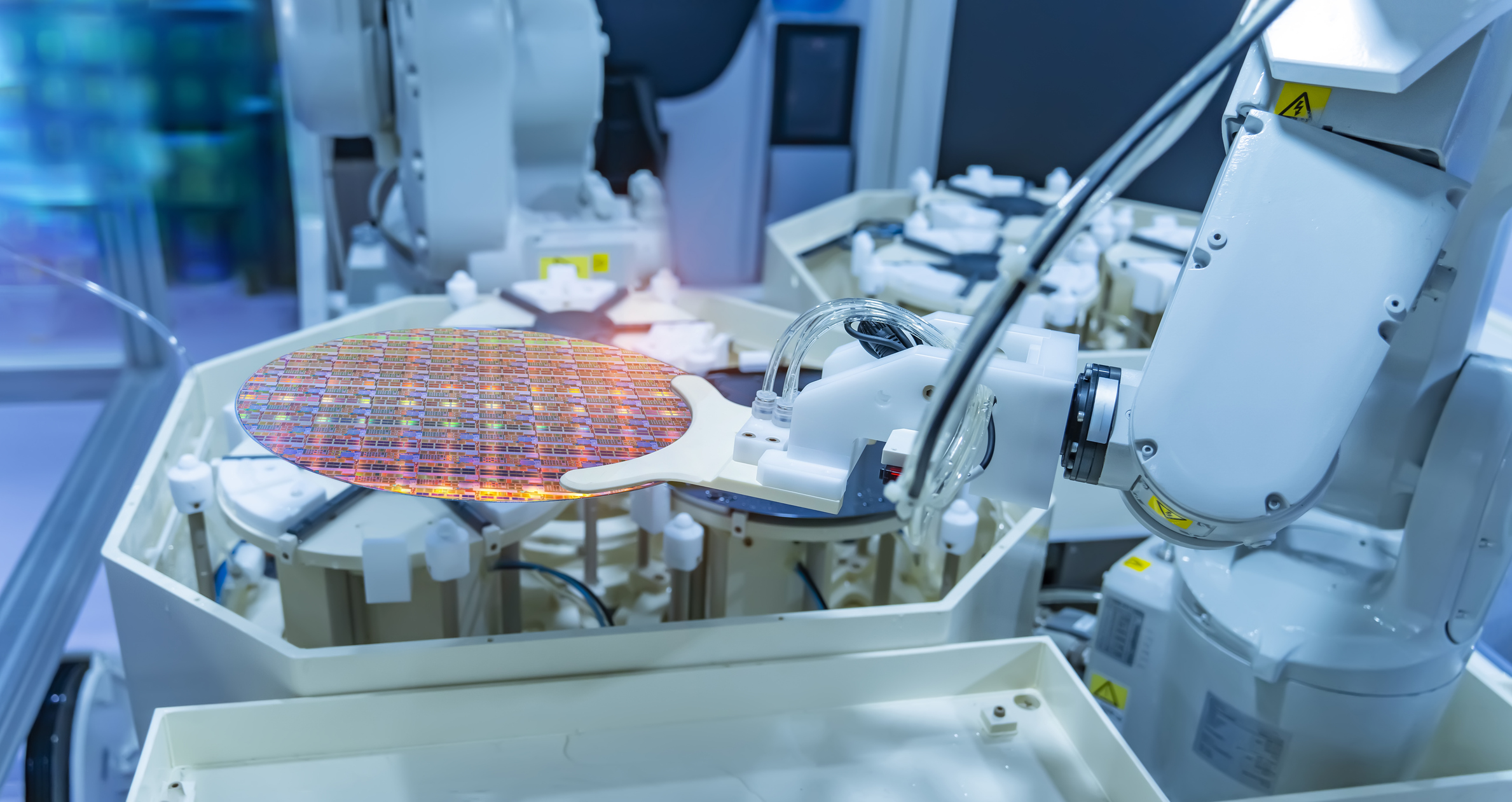
Precision Clamping Pressure
Measure and visualize pressure distribution in wafer clamping and fixturing systems to verify uniform force application, identify misalignment, and reduce the risk of wafer damage during critical process steps.
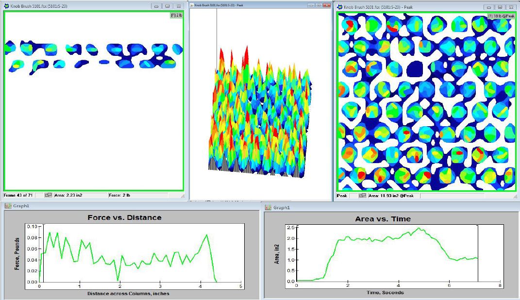
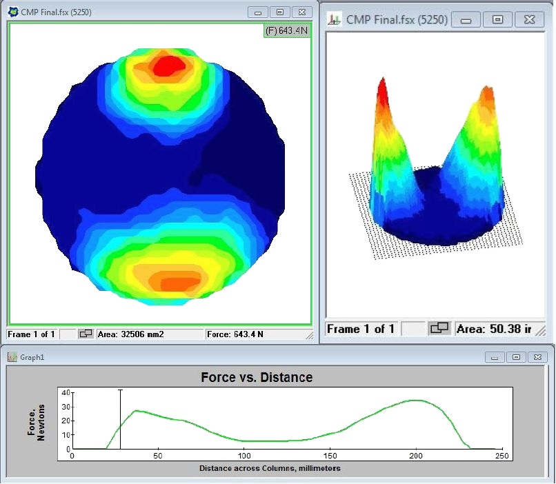
Post-CMP PVA Brush Testing
Assess pressure applied by PVA brushes during post-CMP cleaning to identify uneven contact, reduce defect risk, and validate cleaning tool performance.
Wafer Polishing Evaluation
Evaluate contact and pressure uniformity during wafer polishing processes to improve material removal consistency, optimize pad performance, and support tighter process control.