Semiconductor Clamping Pressure Distribution
Challenge
Unknown clamping forces during computer chip and heat sink mounting or wafer probe testing can cause considerable product defects and quality issues. This can lead to lower yields and increased costs and product waste.
Solution
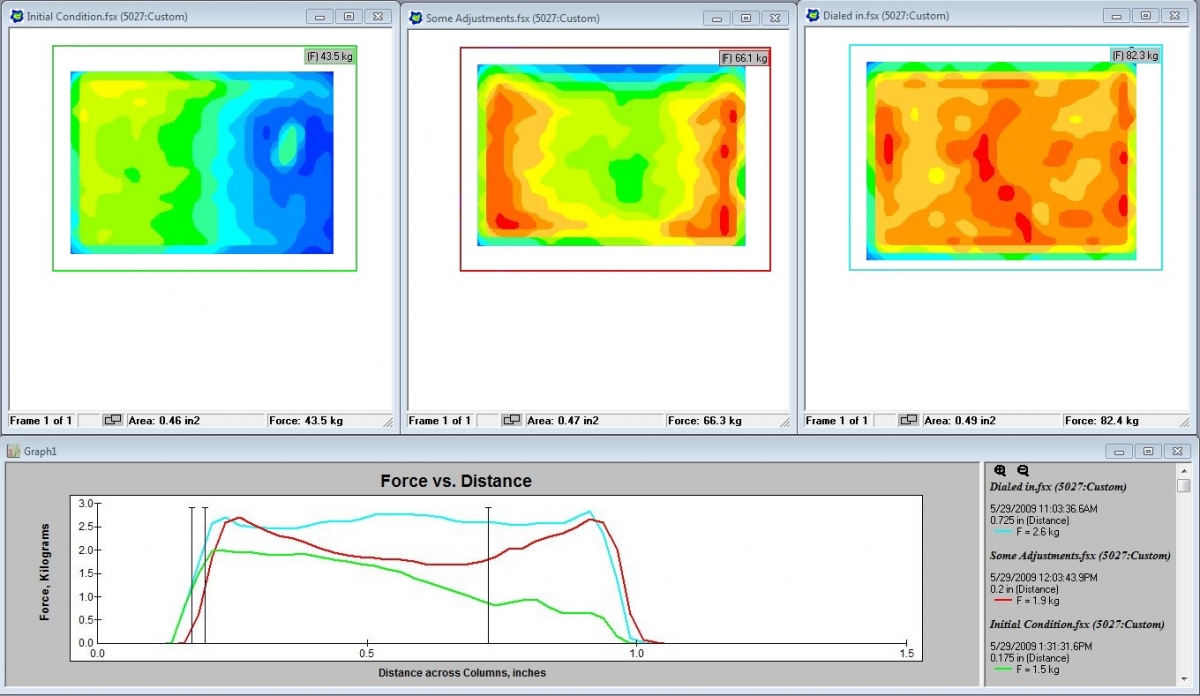
The I-Scan™ force and pressure mapping system is a key diagnostic and machine set-up tool for clamping fixtures. The ultra-thin (0.1 mm) sensors can be placed between any two mating surfaces, such as a heat sink and its heat source or a probe and wafer. The system allows for real-time viewing of the pressure distribution between the clamping fixture and opposing surface.
If the optimal pressure is not achieved, adjustments can be made to optimize the clamping fixture design, quantify forces, or determine ideal protocols such as torque patterns and procedures. The I-Scan pressure mapping system can be used to optimize pressure distribution prior to a testing sequence or production run, saving valuable company time and money. With the help of Tekscan's highly qualified sales and engineering support team, each system can be configured to meet your specific needs.
Semiconductor Clamp Pressure distribution Applications
- Coplanarization
- Research and Development
- Detect defects or obstructions
- Before and after adjustment comparison
- Quality assurance testing
- Machine to machine comparison
- Design verification testing
Benefits of Pressure Mapping
- Better bonds and seals
- Identify low yield machines
- Increase manufacturing yields
- Reduce costs and product waste
- Provides data for improved design
- Less wear and tear on production equipment
- System Flexibility- can adapt to different or changing measurement needs
Gain Insights in the Semiconductor Manufacturing Process
Establishing and maintaining evenness between contacting surfaces is often both crucial and difficult to achieve. For testing and inspection in semiconductor manufacturing, this can be a key factor in order to produce a higher quality, or simply a functional product. Tactile pressure mapping technology from Tekscan gives engineers the insight needed for various applications in this field.
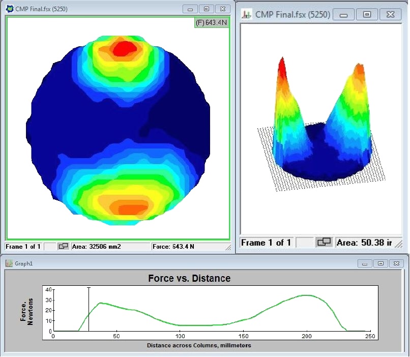 CMP Wafer pressure distribution during polishing process.
- Integrate with 3rd party test equipment for in-depth analysis
- Versatile system with multiple sensors and electronics
- Minimally invasive thin-film sensor
- High-resolution sensors for detailed analysis
- High temperature sensors to collect data under application conditions
- Customizable sensors available
Watch this video to learn more about how Pressure Mapping Technology can help validate component press fits or seals: