Evaluate Brush-to-Wafer Contact Pressure
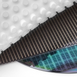
Polyvinyl alcohol (PVA) brushes are used in the semiconductor process during the post-CMP cleaning stage. Different PVA brush designs can affect wafer cleaning efficiency. Ensuring proper brush-to-wafer contact pressure and contact area is crucial in achieving clean and particle free wafers.
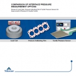
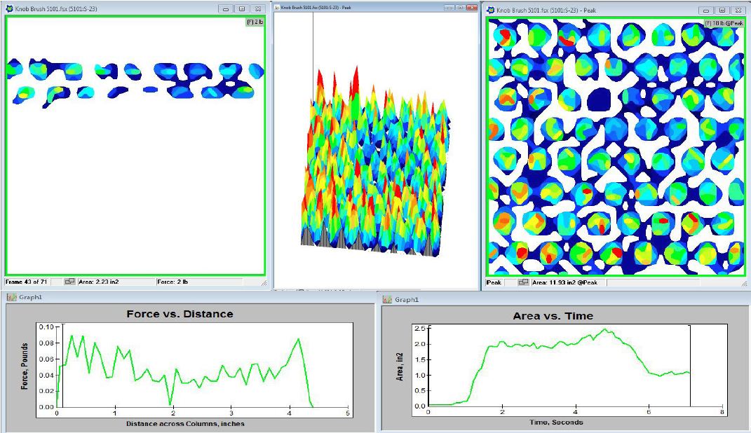
The I-Scan™ pressure and force mapping system and tactile pressure sensors provide immediate feedback on the effectiveness of the brush by measuring the contact pressure distribution and area in real-time, and displaying any pressure inconsistencies in 2D or 3D displays. Adjusting a brush design or implementing different machine set-up parameters can be evaluated and compared, prior to the wafer cleaning run, saving valuable company time and manufacturing costs.
With the help of Tekscan’s highly qualified sales and engineering support team, each system may be configured to meet your specific needs. Learn more about the I-Scan pressure mapping system.
Brush Testing Applications
- Determine proper brush to wafer contact pressure
- Compare brush designs
- Machine set-up and adjustment
- Correlate output quality to set-up
Benefits of Measuring Contact Pressure with Tactile Pressure Sensors
- Ensure consistent wafer cleaning performance
- Improved cleaning consistency
- Reduces machine set-up time
- Increased product yields