
A Solution to Confirm Heat Sink Contact Pressure for Consumer Electronic Devices

Heat sinks are important components that stop consumer electronic devices from over-heating while in use. Even and secure heat sink installation is vital to their function, and pressure mapping can help.
Addressing demands for aesthetics and function can be a challenge when developing consumer electronic devices. Users crave more power and capabilities from their devices, while also demanding that the device will be small, compact, and stylish. However, these competing features pose complications from a design-engineering perspective.
Electronic devices produce heat from their printed circuit board (PCB) components when in use. The smaller and more compact the device becomes, the greater the chances these heat-producing components will damage the device over time. Therefore, the designer should account for a way to manage excessive heat produced by PCB components.
Installing cooling fans within the device is one option, but because they take up a lot of space – and require extra power to function – this may not be acceptable for many types of consumer devices.
Heat sinks are a common cooling alternative for consumer electronics that cannot accommodate fans, or other direct-cooling methods. Heat sinks are passive cooling elements typically made from aluminum or copper that are secured to heat-producing PCB components. Heat sinks come in many different designs and sizes, including ones small enough to fit within handheld devices, like smart phones, gaming systems, and wearable electronics.
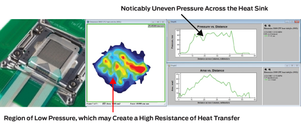 Figure 1: With an I-Scan™ pressure mapping sensor inserted between a heat sink and a mating surface, designers can capture important insights on heat sink contact, and make adjustments if needed.
For a heat sink to function properly, they must be installed evenly and securely to the heat source. Because of the rigid nature of these mating components, even and secure heat sink installation can be difficult to achieve repeatedly, which is important when producing consumer devices in high volumes.
Pressure mapping technology has proven to be a useful tool to help with verifying heat sink contact to a PCB or component. As shown in Figure 1, the paper-thin pressure sensors can be inserted between the heat sink and PCB component to:
- Measure the real-time contact pressure while installing the heat sink
- Monitor pressure results before and after changes are made in the manufacturing process (Figure 2)
- Help in the heat sink material-selection process, as well as the design of the clamshell fixture holding the heat sink in place
- Provide quantifiable data for quality control procedures
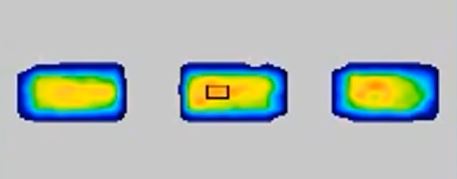 Figure 2: This image displays pressure output from a heat sink after different adjustments in the manufacturing process. The pressure feedback on the right clearly displays lesser pressure uniformity toward the bottom, while the middle image shows excessive pressure toward the center.
Correlate Heat Sink Pressure and Temperature Changes
Now with temperature mapping, you can track both surface temperature and pressure data at the same time. Temperature mapping data can give you key R&D insights in semiconductor design and engineering, as well as manufacturing, battery design, packaging and more.
How Else Can Pressure Mapping Help in the Design of Consumer Electronic Devices?
The eBook presents examples on the contributions that Pressure Mapping has made in helping the electronics & semiconductor industry to gain the insight needed for various applications and processes in this field.