
Proving a Proper Component Fit or Seal
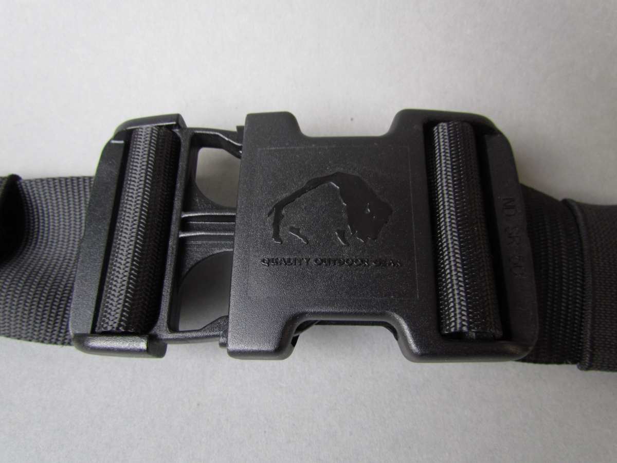 Isn’t it satisfying when two connecting parts *snap* perfectly into place? Single moments like the *click* of a buckle or a padlock, and even the *pop* a sealed jar makes when opened for the first time, are clear audible indicators of a robust and secure product design. For design engineers of these types of products, these moments help validate standards for fit and contact.
For lots of other products though, this *snap* moment isn’t so clear.
Achieving proper fit between two mating surfaces can be difficult. Peak pressures may be "hiding" between your mating surfaces, even if a "good fit" seems apparent. In many manufacturing environments, common methods used to confirm a secure or uniform part fit may not be telling the full story. In some cases, the slightest pressure imbalance in the manufacturing process can result in product failure.
However, pressure mapping can be a powerful technology to uncover peak pressure by capturing dynamic insight on component fit and contact in seemingly unreachable spaces. Here are some recent successes:
|
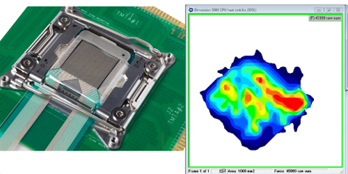
Evaluating & Improving Heat Sink Contact Heat sinks are components administered to circuit boards to help keep electrical systems from overheating. Because of a mechanically “stiff” nature of the heat sink and hard surfaces involved, there can be potential contact gaps, especially across larger areas. In this application, pressure mapping sensors were positioned between the heat sink and a circuit board to provide quantitative overview of the contact area. Engineers used this data to tweak their heat sink application process to ensure the best coverage of sensitive electrical components. |
|
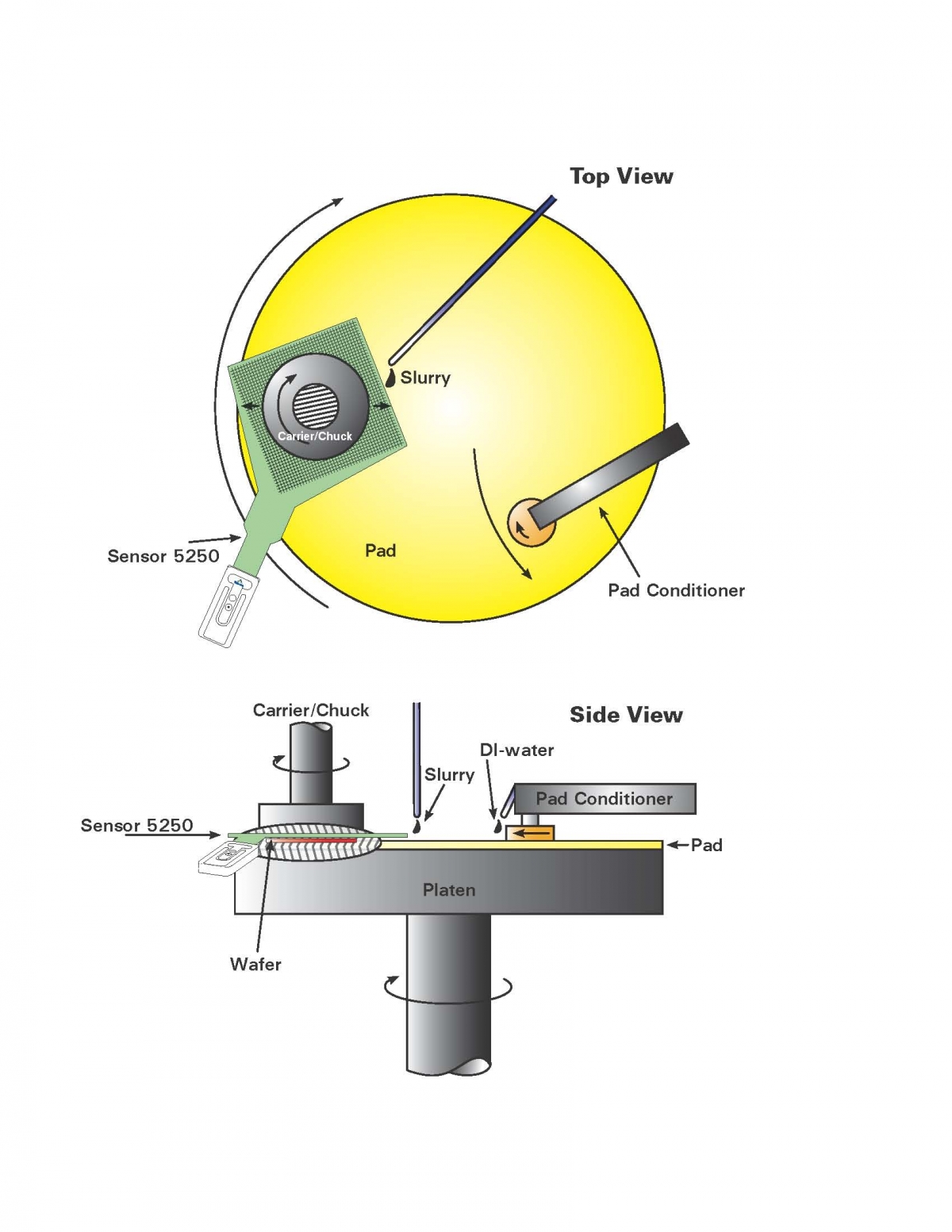
Commanding Greater Control in Semiconductor Testing Semiconductor testing operations use pick & place systems to handle highly sensitive components. These systems are programmed to execute extremely calculated movements with exact precision. However, these systems are not perfect – inconsistencies that can occur during the wafer polishing process may prompt product defects. Pressure mapping technology has been used in chemical mechanical polishing operations to obtain insight into the pressures applied by a polishing head onto a wafer during the testing process. Sensors laid over the top of a wafer were used to measure the contact pressure to identify uneven polish, worn parts, and low pressures, which would ultimately help minimize product waste. |
|
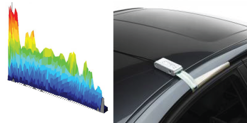
Demonstrating a Secure, Sealed Operating Environment Extreme temperatures, wind, moisture, and general wear & tear can take its toll on door latches and seals. In the past, vehicle assembly technicians would ultimately have to guess where to position hinges and latches that would provide the best long-term seal over the vehicle’s time in surface. With pressure mapping, technicians can obtain clear visual feedback on where peak pressures exist between a door and the rubber seal of the vehicle. This helps them develop a “gold standard” for positioning the door components that provides maximum protection, durability, and superior driver/passenger comfort. |
For design engineers seeking that *snap* feeling for a proper fit or seal, pressure mapping technology may be able to provide you with something even better: quantifiable proof of a well-designed product or device.
Let’s discuss your design challenge – contact our sales engineers today.
Post Categories: