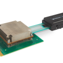
Evaluate Heat Sink Contact Pressure Background High density, active, electronics emit energy that can raise their temperature leading to failures. Heat sinks are secured to components to dissipate their heat. Challenge For the heat sink to function properly, even contact must be achieved between the...

Pressure Mapping for the Semiconductor Industry

Measuring Pressure Distribution During the Semiconductor Process

Perform Real-time Pressure Measurements During Semiconductor Design and Manufacturing Process


Throughout all aspects of semiconductor manufacturing, constant testing and inspection are necessary to yield high quality and functioning products. The I-Scan™ System from Tekscan enables engineers and machine operators to quickly and accurately perform real-time pressure measurements during the various stages of the semiconductor process.
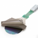
Wafer Polishing Pressure Measurement Wafer or Chemical Mechanical Polishing (CMP) requires that an even surface is achieved or subsequent manufacturing steps will be adversely affected, costing your company money. The I-Scan™ pressure mapping system provides instantaneous insight into the pressures...

Semiconductor Clamping Pressure Distribution Challenge Unknown clamping forces during computer chip and heat sink mounting or wafer probe testing can cause considerable product defects and quality issues. This can lead to lower yields and increased costs and product waste. Solution The I-Scan™ force...

Evaluate Brush-to-Wafer Contact Pressure Polyvinyl alcohol (PVA) brushes are used in the semiconductor process during the post-CMP cleaning stage. Different PVA brush designs can affect wafer cleaning efficiency. Ensuring proper brush-to-wafer contact pressure and contact area is crucial in...