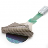
Wafer Polishing Pressure Measurement
Wafer or Chemical Mechanical Polishing (CMP) requires that an even surface is achieved or subsequent manufacturing steps will be adversely affected, costing your company money.
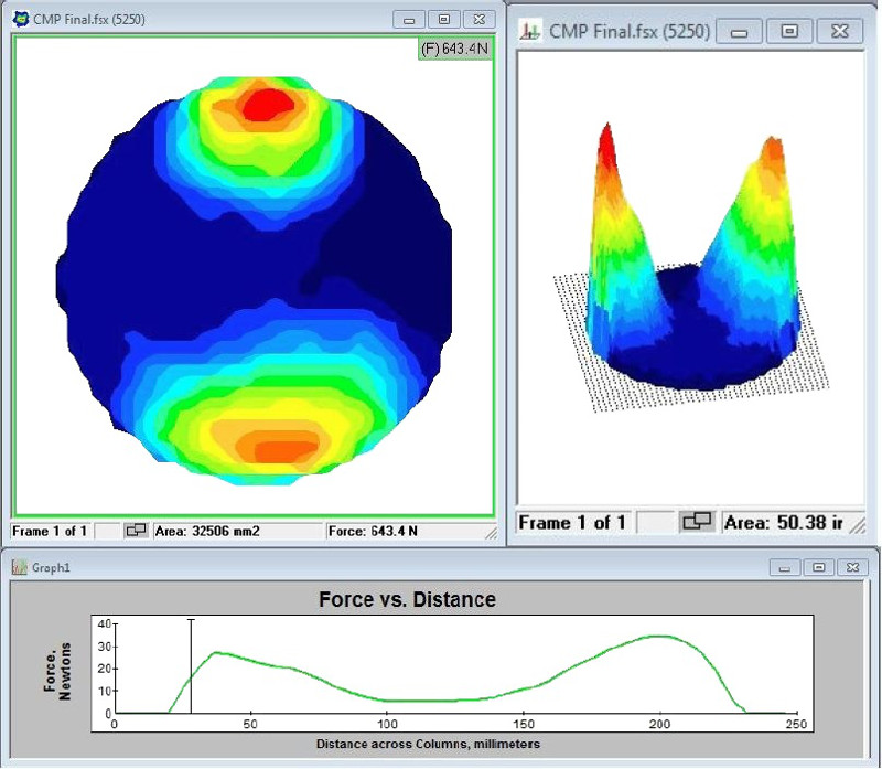
The I-Scan™ pressure mapping system provides instantaneous insight into the pressures applied by a polishing head on a wafer during the polishing process. If uneven pressures exist, the I-Scan will display them in colorful 2D and 3D images. Machine adjustments can then be made and new measurements taken to ensure even pressure.
The patented thin sensors easily fit in this application and minimize environmental disturbance thus measuring the true pressure pattern. Sensors are available in different shapes, are reusable, and provide accurate pressure readings. With the help of our highly qualified sales and engineering support team, each system may be configured to meet your specific needs.
Wafer Polishing Pressure Measurement Applications
- Identify uneven polish, worn parts, and low pressures
- Before and after adjustment comparison
- Machine to machine comparison
- Reliability and validation testing
Benefits of Pressure Mapping
- Improves machine set-up:
- Save time & money
- Minimize product waste
- Identify low yield machines
- Increase manufacturing yield


